<img height="1" width="1" style="display:none;" alt="" src="https://px.ads.linkedin.com/collect/?pid=9163618&amp;fmt=gif">
Images_sample prep_

Sample Preparation
& Cleaning Systems

Ion milling and UV sample cleaning for high-quality electron microscopy

Sample preparation is where electron microscopy results are won or lost. Mechanical damage and hydrocarbon contamination degrade your image, while also wasting your time on the microscope.

Hitachi's sample preparation and cleaning systems are designed to solve this. From high-precision ion milling to gentle UV-based contamination removal, these tools help you get cleaner surfaces, sharper images, and more reliable results.

Ion milling systems

IM4000II & IM5000
Broad argon ion milling for artifact-free SEM sample preparation

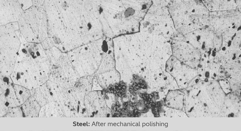
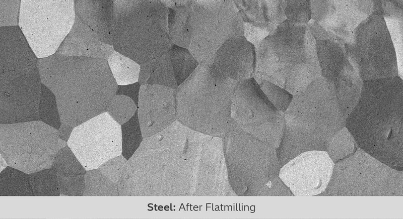
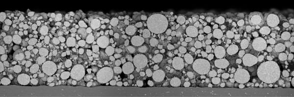
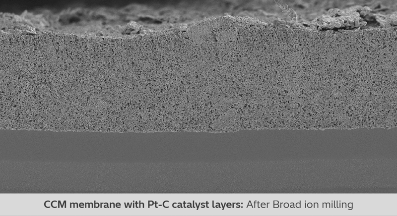
Mechanical polishing introduces smearing and deformation. Ion milling doesn't. The IM4000II and IM5000 use a broad argon ion beam to remove material layer by layer. So you get pristine cross-sections and polished surfaces that reveal the true microstructure of your sample.

Whether you're working with metals, semiconductors, polymers, ceramics, batteries, or multilayer structures, these systems deliver smooth, stress-free surfaces ready for SEM, EDS, and EBSD analysis.

Images_sample prep_2_transparent
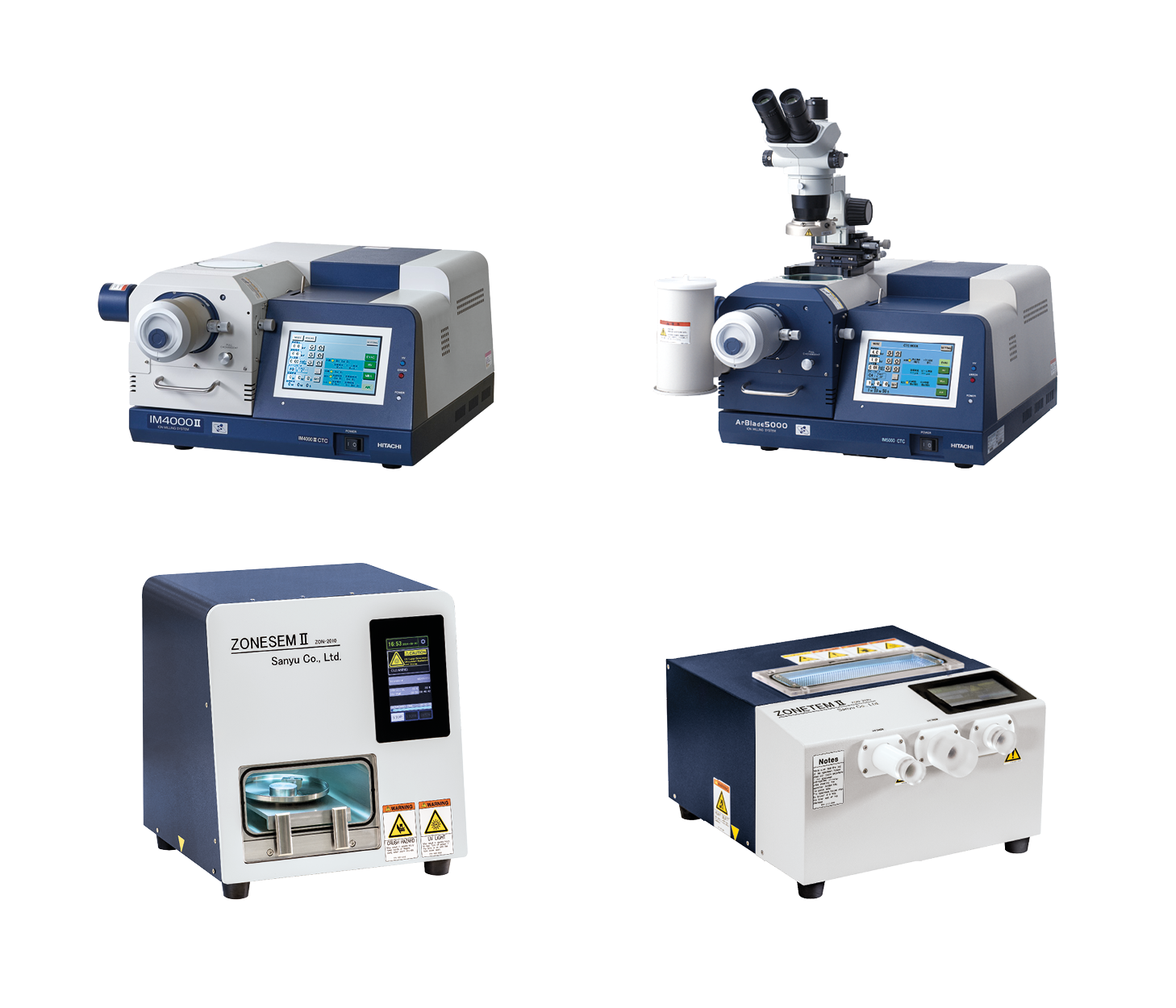
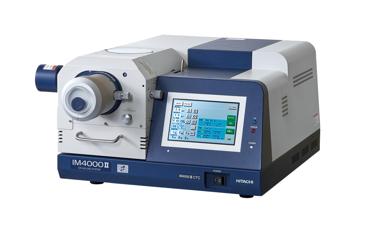
  • IM4000 II: A flexible all-in-one system for cross-section and flat milling. Ideal for labs that need a versatile, everyday sample prep tool.
Images_sample prep_3_transparent
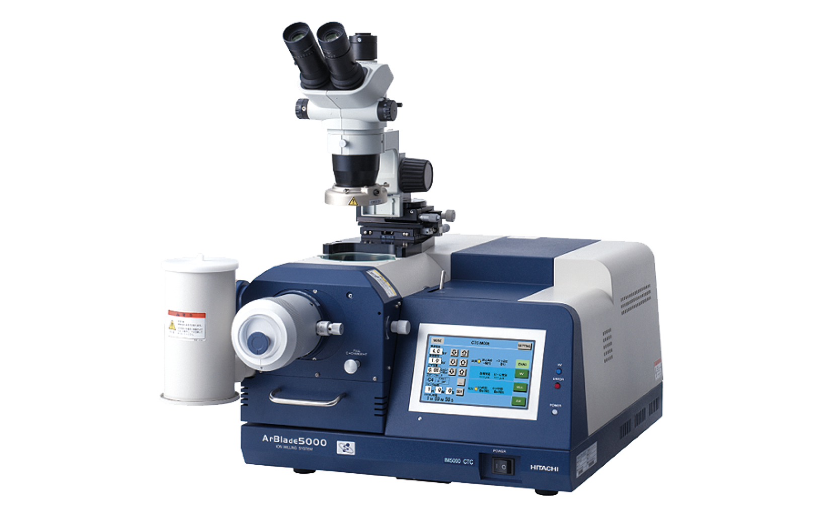
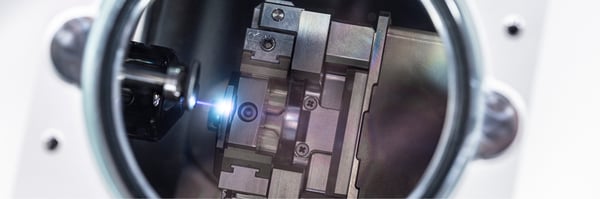
  • IM5000: Higher milling rates and wide-area cross-sectioning (up to 10 mm width) for demanding applications and higher throughput.
Why labs choose the IM4000II or IM5000 over mechanical prep

Explore the IM4000II & IM5000 in detail

Specifications

Ion milling systems IM4000II IM5000
Gas Used Argon Argon
Accelerating Voltage 0 to 6 kV 0 to 8 kV
Maximum Milling Rate (Si, 100 μm protrusion) ≥500 μm/h ≥1 mm/h*
Maximum Milling Width 1,4 mm 10 mm
Maximum Specimen Size 20(W) × 12(D) × 8(H) mm 20(W) × 12(D) × 8(H) mm
Sample Moving Range X: ±7 mm, Y: 0 to +3 mm X: ±7 mm, Y: 0 to +3 mm
Intermittent milling ON/OFF (1 sec–59 min 59 sec) ON/OFF (1 sec–59 min 59 sec)
Swing angle ±15°, ±30°, ±40° ±15°, ±30°, ±40°
Wide-Area Cross-Section milling No Yes
Flat Milling Area φ 32 mm φ 32 mm
Max. Flat-Milled Sample Size φ 50 x 25(H) mm φ 50 x 25(H) mm
Rotation Speed (Flat Milling) 1 rpm, 25 rpm 1 rpm, 25 rpm
Tilt Range (Flat Milling) 0–90° 0–90°
Cryogenic cooling (optional) Yes Yes
Higher Beam Tolerance Mask (optional) 2x beam tolerance (Cobalt-free) 2x beam tolerance (Cobalt-free)
Stereo Microscope Unit (optional) 15x to 100x, Binocular/Trinocular 15x to 100x, Binocular/Trinocular

*For Si sample with protrusion of 100 μm

UV sample cleaners

ZoneSEMII & ZoneTEMII
Chemical-free hydrocarbon removal for cleaner SEM and TEM imaging

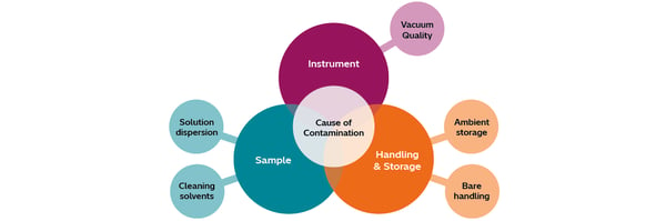
Hydrocarbon contamination is one of the most common causes of poor image quality in electron microscopy. Whether it builds up during preparation or accumulates during imaging, carbon-based residue obscures fine detail, distorts EDS data, and wastes valuable microscope time.

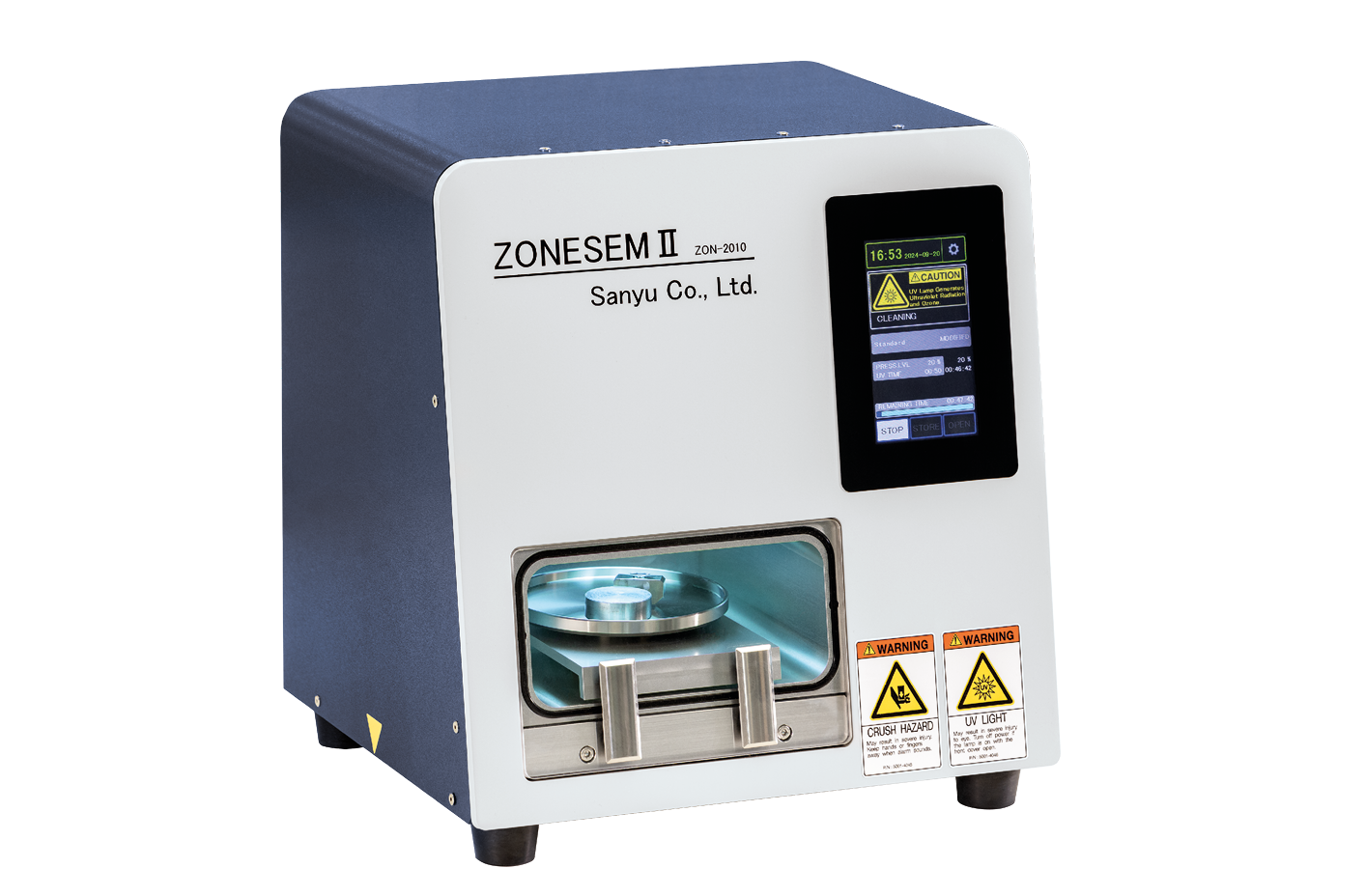
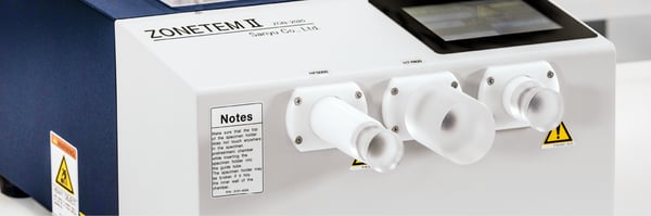
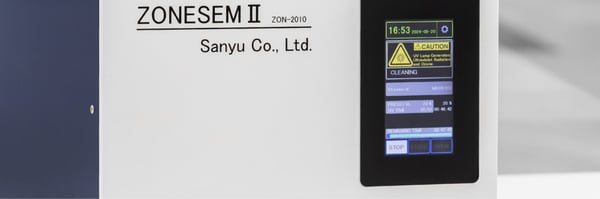
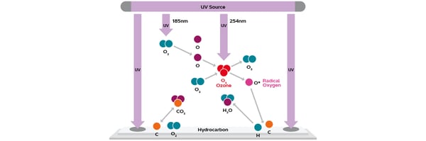
The ZoneSEMII and ZoneTEMII use low-energy UV light and activated oxygen to break down and remove hydrocarbon contamination. Gently, quickly, and without chemicals, solvents, or gas supplies.

Images_sample prep_4_transparent
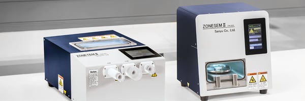
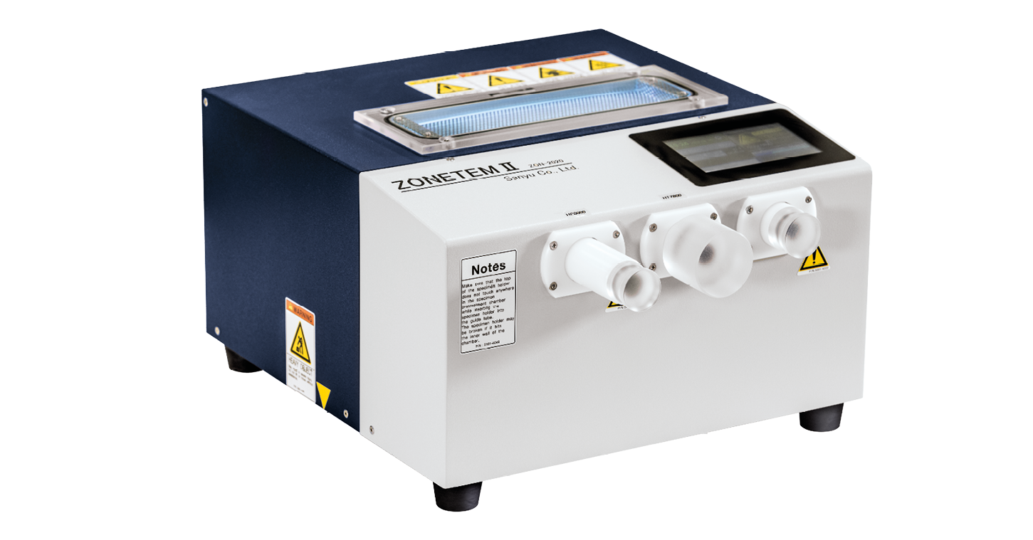
  • ZoneSEMII: Designed specifically for SEM sample holders (optimized for Hitachi holders). Cleans and stores samples to prevent re-contamination before imaging.
Images_sample prep_5_transparent
  • ZoneTEMII: Designed for TEM grids and holders. Removes hydrocarbon contamination from delicate specimens ahead of high-resolution TEM/STEM work.
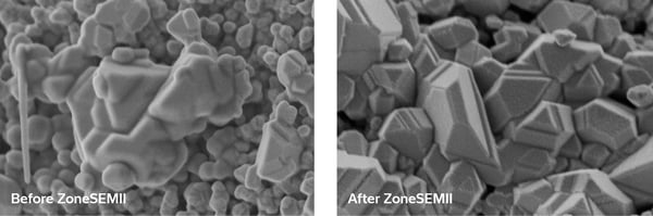
Why labs use ZoneSEMII or ZoneTEMII for UV sample cleaning

Explore the ZoneSEMII & ZoneTEMII in detail

Specifications

UV Sample Cleaners ZoneSEMII ZoneTEMII
Cleaning method UV light + activated oxygen UV light + activated oxygen
Target application SEM samples and holders TEM grids and holders
Holder compatibility Optimized for all SEM holders TEM specimen holders, also for other manufacturers
Vacuum control Adjustable Adjustable
Interface Touchscreen with recipe memory Touchscreen with recipe memory
Storage function Yes — clean and store in one unit Yes — clean and store in one unit
Chemical/gas requirements None None
Footprint Compact, desktop Compact, desktop

Applications gallery

Applications_Sample prep_1

Applications_Sample prep_2

Prepare cross-sections for microstructural analysis without mechanical deformation.
Applications_Sample prep_3

Applications_Sample prep_4

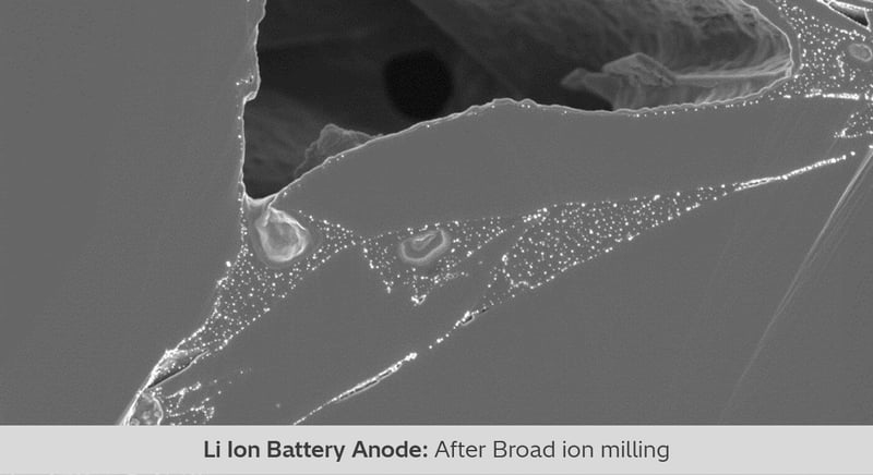
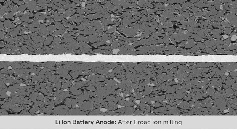
Mill electrode cross-sections and transfer samples to the SEM without air exposure, preserving sensitive interfaces.
Applications_Sample prep_5

Applications_Sample prep_6

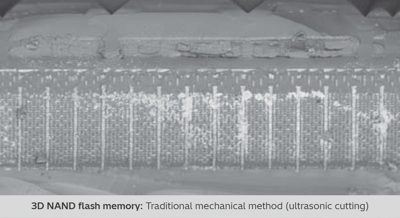
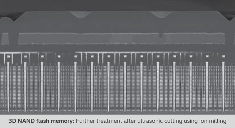
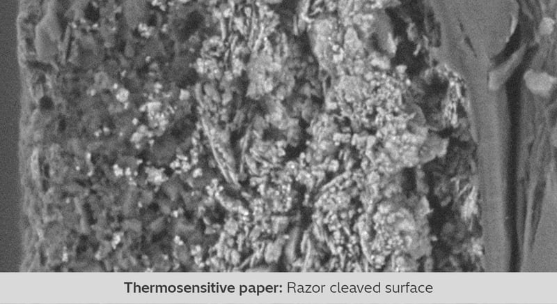
Expose layers, interfaces, and defects in ICs, PCBs, and multilayer devices.
Applications_Sample prep_7

Applications_Sample prep_8

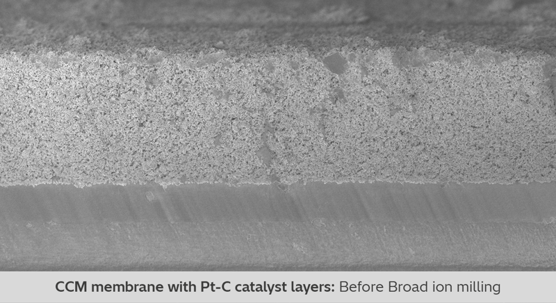
Use cryogenic cooling to prevent thermal damage during ion milling, and UV cleaning to remove hydrocarbon residue before imaging.
Applications_Sample prep_9

Applications_Sample prep_10

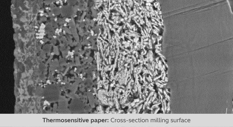
Study layer composition and adhesion quality without introducing delamination or smearing.
Applications_Sample prep_11

Applications_Sample prep_12

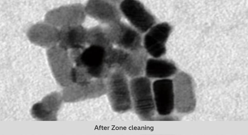
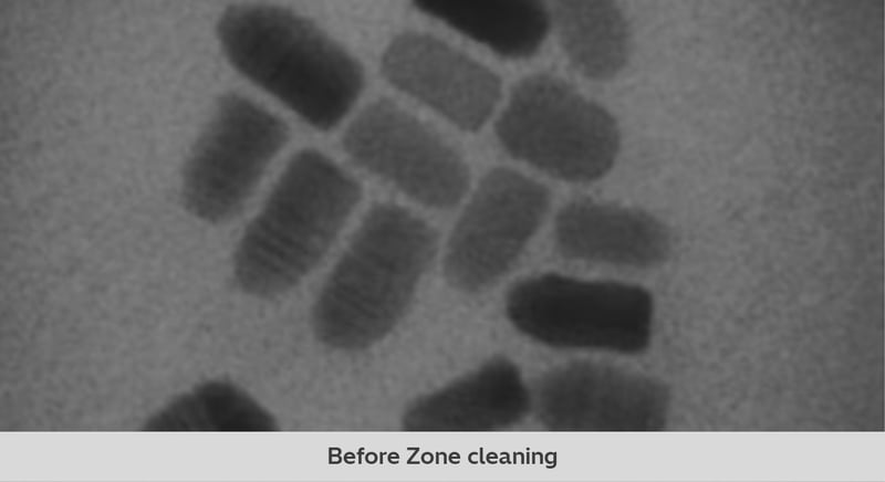
Remove hydrocarbon contamination from TEM grids for sharper, more reliable high-resolution data and EDS mapping.

Contact us

Whether you're setting up a new sample prep workflow or looking to improve the quality of your existing results, our specialists can help you choose the right sample prep tools. Contact a Hitachi specialist today.