
SU8600
Cold Field Emission SEM
The CFE-SEM for ultra-high spatial resolution, multi-perspective imaging
- Ultra-high resolution of 0.6 nm at 15 kV and 0.7 nm at 1 kV.
- Advanced automation for consistent, repeatable workflows.
- Display up to six imaging signals at the same time.
- Fast and easy specimen loading through standard six inch exchange chamber.
Overview
The SU8600 is a dedicated imaging SEM offering ultra-high resolution thanks to Hitachi’s cold field emission (CFE) technology. Designed to meet the needs of research scientists, lab managers, and industrial users alike, the SU8600 CFE-SEM delivers excellent spatial resolution and automation for modern labs.
1, 2, 4 or 6 signals can be displayed at the same time on a single monitor. By adding a second screen, the dual-monitor configuration boosts productivity and expands your workspace. Dual monitors also allow you to customise the operation panel with submenus positioned anywhere on either screen.
Features and benefits
-
Ultra-high resolution for unmatched imaging
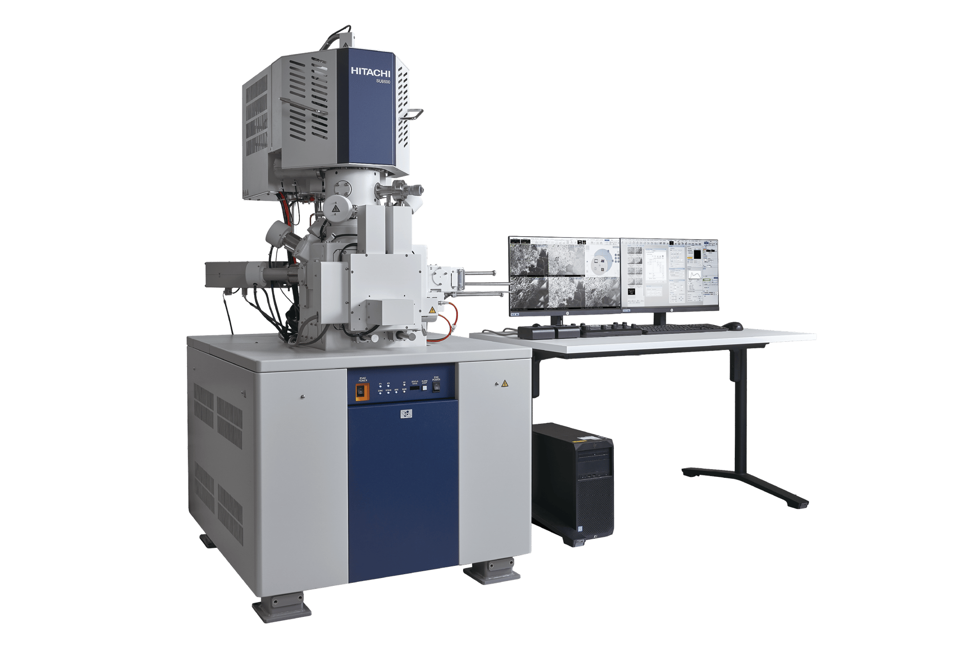
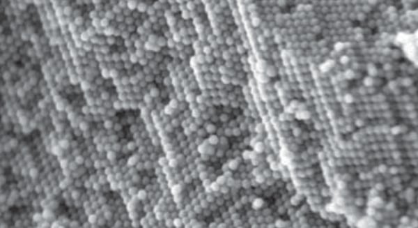
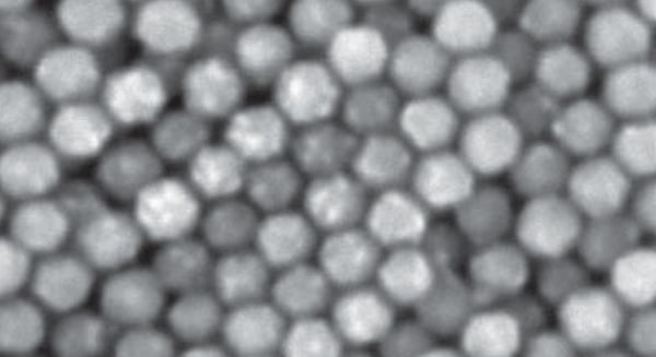
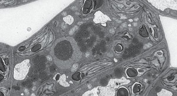
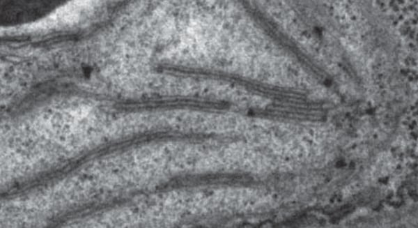
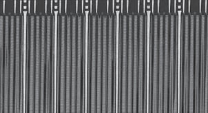
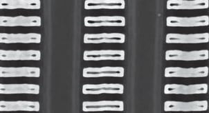
The SU8600’s high-brightness cold-field emission source provides exceptional resolution, even at low voltages. This lets you capture intricate details with clarity, making it ideal for advanced material science, semiconductor studies, and biological analysis.
The narrow energy width (almost monochromatic) emission minimizes chromatic aberrations, so you can operate the SU8600 without beam boosting.
Multiple signals emitted from the observed specimen are collected by the magnetic lens field and guided into the in-column, multi-detector system. This system lets you display up to six imaging signals at the same time.
-
Smart detector system for better contrast
The Out-Column Crystal Type BSED (OCD) enables fast backscattered electron imaging (BSE), capturing structural details in under one second. So you save time while distinguishing material differences with precision, such as oxide and nitride layers in semiconductors.
That’s not all. High-pass filtering for elastically backscattered electrons allows material contrast imaging without deep beam penetration. You’re able to maintain sample integrity while observing surface-level features, crucial for delicate specimens or beam-sensitive materials.
Energy filtering also gives you the following benefits:- You can easily suppress image charging by selecting faster, non-charge-affected electrons.
- You can image surfaces with different conductivities, e.g. doping regions in semiconductors.
- You can image SE or filtered-SE (fine surface detail) or elastically backscattered electrons (material contrast information) at the same time.
- You can apply a window-less EDX system at all accelerating voltages, since the magnetic field prevents backscattered electrons from hitting the EDX detector where they would cause spectrum background.
-
Enhanced automation for reproducibility
The optional EM Flow Creator software lets you use a “drag and drop” method to configure SEM operations into repeatable workflows. Once a recipe is configured, automated data collection under set conditions can be done with high accuracy and repeatability. So you get consistent results with minimal manual intervention, which is perfect for labs managing high-throughput experiments.
-
Flexible and user-friendly design
Display up to six signals at the same time on a single monitor so you can analyze data efficiently. Or use a dual monitor configuration to expand your workspace with extra display options.
The standard six-inch specimen exchange chamber with optional inert-gas transfer mechanism lets you minimize contamination risks while accommodating a wide variety of sample types.
Using the exchange chamber lets you keep the chamber permanently under vacuum, ensuring minimal background contamination. The stage itself boasts a 110 mm x 110 mm range of motion in X and Y.
Specifications
Electron Optics | |
Resolution | 0.6 nm @ 15 kV, 0.7nm @ 1kV |
Magnification | 20 to 2,000,000x |
Voltage Range | 0.5 to 30 kV |
Specimen Stage | |
Stage Control | Motorized 5-axis control |
X/Y/Z range | 0–110 mm / 1.5–40 mm |
Tilt | -5° to 70° |
Detectors | |
Standard Detectors | Optional Detectors |
Upper Detector (UD) | Top Detector (TD) In Column Middle Detector (IMD) Photo Diode BSE (PD-BSE) Out Column Detector (OCD) Bright Field TE (BFSTEM) Dark Field TE (DFSTEM) Cathodoluminescence Detector (CL) EDX, EBSD |
Lower Detector (LD) | |
Optional Accessories | EDX and EBSD |
Applications gallery


Self Assembling Magnetic Iron Oxide Nanoparticles


Ultrastructure of Arabidopsis


Cross Section Images of 3D NAND
Contact us
Our specialists are here to guide you in selecting the right SEM for your needs. Reach out to learn how the SU8600 can enhance your lab’s imaging capabilities, streamline workflows, and support your scientific or industrial applications.