Features_SU3800SE_SU3900SE_1

SU3800SE and SU3900SE

Advanced SEMs for fast, high-quality imaging and automated workflows

Powerful, versatile SEMs designed for performance, large-sample handling, and user-friendly automation imaging needs in academia and industry.

Why choose the SU3800SE and SU3900SE?

The Hitachi SU3800SE and SU3900SE scanning electron microscopes give you an imaging and analytical solution for a wide range of applications. These instruments deliver high-resolution imaging, easy sample navigation, and advanced automation features - offering reliable, consistent results across different use cases. Whether you need to handle standard samples or larger industrial materials, these SEMs give you the versatility and stability to support your lab’s goals. Ideal for both research labs and industrial environments, the SU3800SE and SU3900SE help reduce time to data, enhance productivity, and ensure reproducible results.

Features and benefits

Specifications

  SU3900SE/SE Plus SU3800SE/SE Plus
Electron Optics
Secondary Electron Image Resolution 0.9nm@30kV
2.5nm@1kV
1.6nm@1kV (*1) (*2)
Magnification 5~600,000×
Electron Gun ZrO/W Schottky Emitter
Accelerating Voltage 0.5kV~30kV
Landing Voltage (*1) (*2) 0.1kV~2kV
Detectors
Standard Detectors Secondary Electron Detector (SED)
TOP detector (TD) (*2)
4+1-segment Semiconductor Type Backscattered Electron Detector (BSED)
Optional Detector (*3) Ultra Variable Pressure Detector (UVD)
Specimen Stage
Stage Control 5-axis Motor Drive
X range 0~150mm 0~100mm
Y range 0~150mm 0~50mm
Z range 3~85mm 3~65mm
Tilt -20~90°
Rotation 360°
Specimen Chamber
Mountable Specimen Size Max. φ 300mm Max. φ 200mm

Applications gallery

Applications_SU3800SE_SU3900SE_1
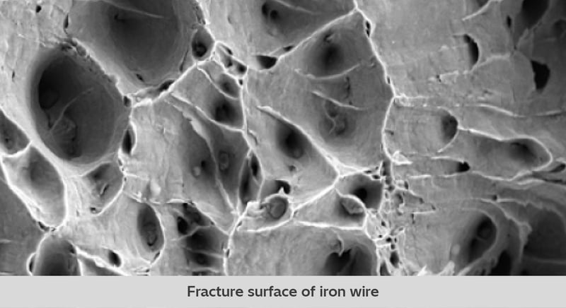
Microcavitation due to ductile failure can be seen.
Applications_SU3800SE_SU3900SE_2
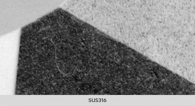
Line-like contrast suggestive of dislocations can be seen.
Applications_SU3800SE_SU3900SE_3
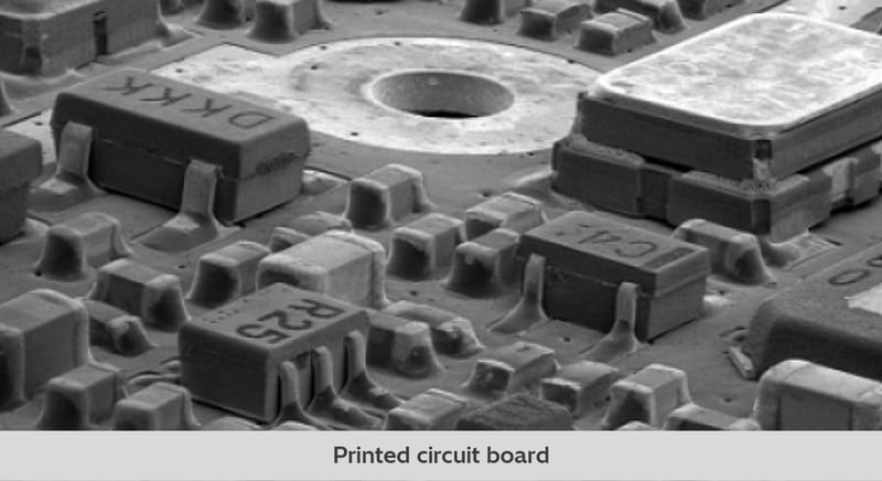
The 3D shapes and positions of mounted components can be seen using low magnification/high-tilt observation.
Applications_SU3800SE_SU3900SE_4
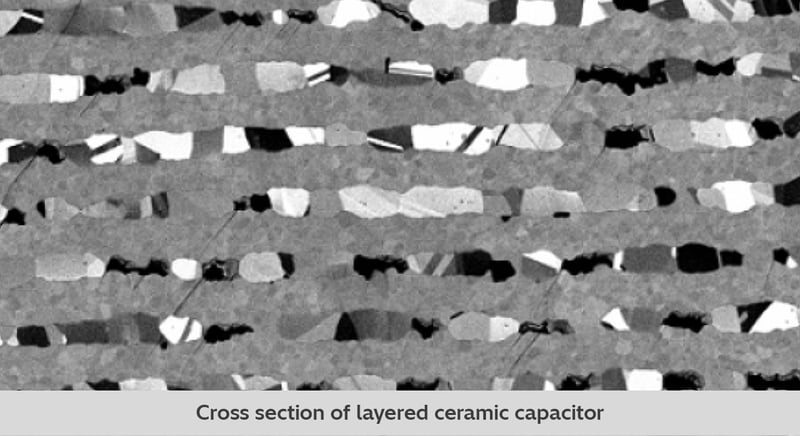
The composition and crystal contrast of nickel electrodes/dielectric layer can be observed.
Applications_SU3800SE_SU3900SE_5
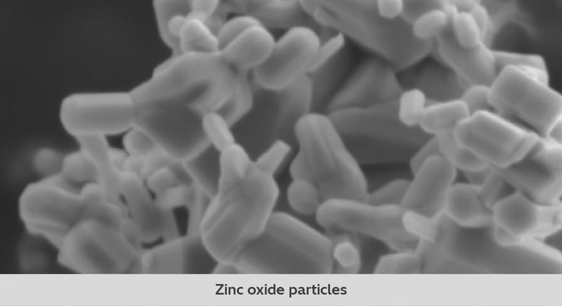
Fine particles with sizes of about 50nm and 3D shape can be seen.
Applications_SU3800SE_SU3900SE_6
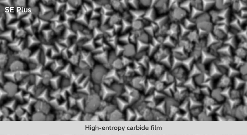
Distribution of particles with different compositions/shapes can be seen.
Applications_SU3800SE_SU3900SE_7
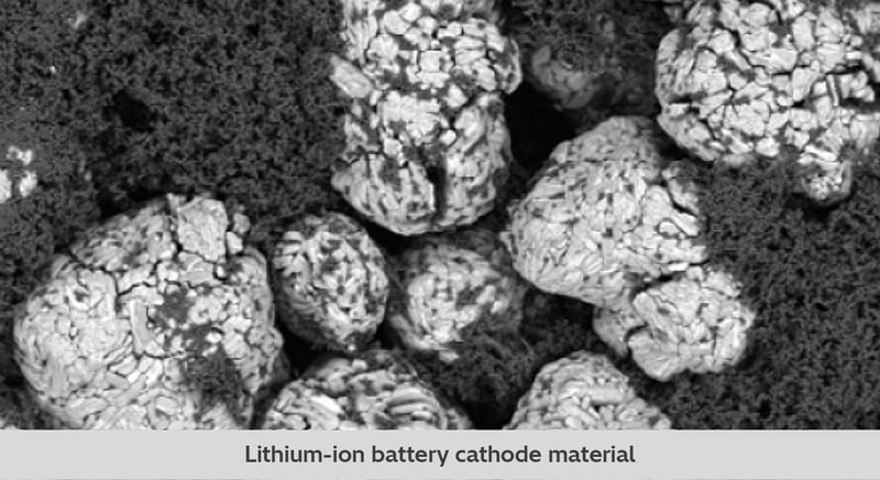
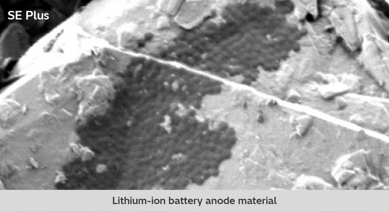
Distributions of cathode material particles and surrounding binder can be seen.
Applications_SU3800SE_SU3900SE_8
Lithium-ion battery anode material and binder is clearly distinguished using static voltage contrast.

Contact us

If you would like help choosing the best SEM for your needs, or if you’re looking for advice on how to optimise your microscopy, our experts are ready to assist. Contact us today to learn how the Hitachi SU3800SE and SU3900SE can enhance your lab’s capabilities.