

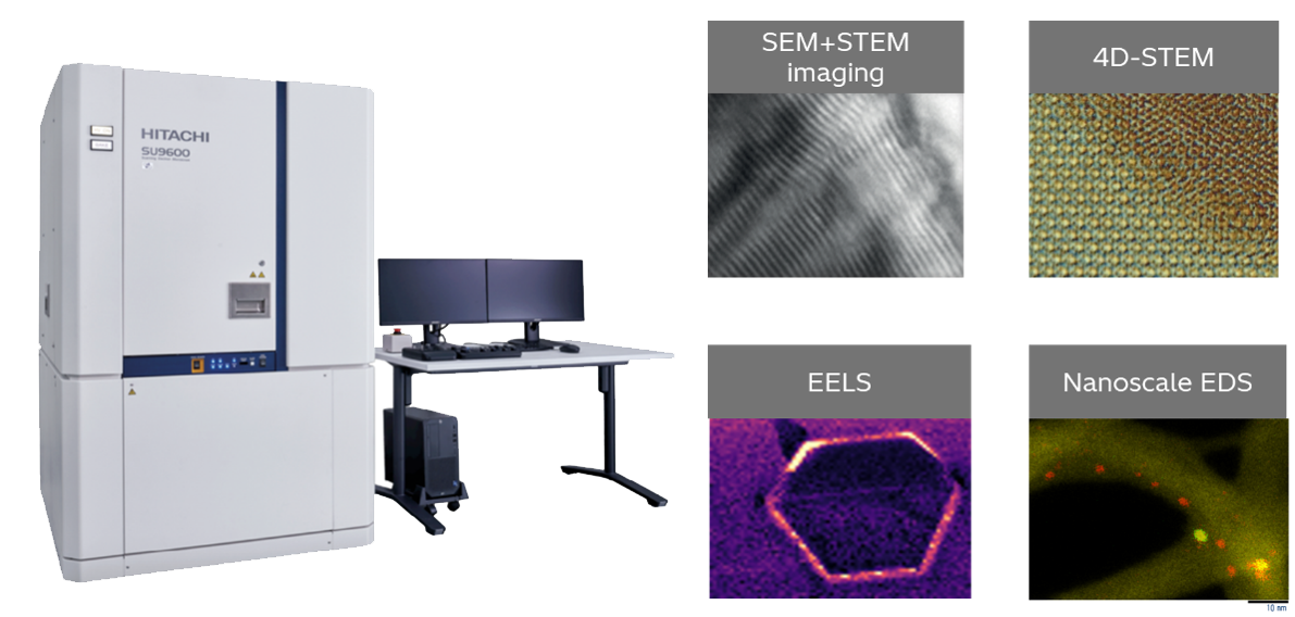
HT7800II 120kvTEM
High-performance 120kV TEM imaging made easy, including tomography and cryo capabilities. The instrument will be equipped with an Oxford EDX and an EMSIS camera.
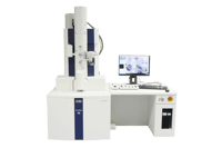
IM5000 broad ion beam (BIB)
Overcome the speed limitations of your FIB and reveal low damage cross-sections up to 40mm wide, giving you more data for more reliable analysis.
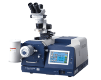
SU3900SE Schottky VP-SEM
Handle the largest specimens and automate complex tasks with the help of Hitachi’s powerful EM Flow Creator.
(Located at the Bruker Booth 125)
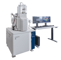
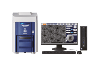
TM4000PlusIII
The latest generation of Hitachi’s popular tabletop SEM brings new capabilities with super-fast EDS and powerful automation.
Tuesday 1st September
EM Flow Creator: Electron Microscope Scripting and Automation Software
Dr. Thomas Schmidt, Manager Applications at Hitachi High Tech Europe GmbH - Booth 149
Bio
Dr Schmidt holds a Diploma in Biology and Biotechnology (University of Münster) and a PhD in Biotechnology and Biochemistry of Plants (Biology, University of Münster). After 5 years as a Postdoc and Head of department at the Leibniz Institute in Aachen, he has been the European applications specialist for TEM and IM at Hitachi-High-Tech Europe for 11 years.
Multimodal low kV STEM
Professor Quentin Ramasse, SuperSTEM Laboratory & University of Leeds
Lunchtime Workshop - Room 20/21
What you will learn
- Pros and cons of pushing analytical capabilities towards high spatial resolution on an SEM platform
- Practical examples of high-resolution EELS and imaging in (T)SEM
- Preliminary demonstration of 4D-STEM capabilities with a high-speed detector
Details
This presentation will illustrate the versatility of high-resolution scanning electron microscopes (SEMs) in a transmission geometry – or (T)SEMs for analytical materials science. Despite the operational simplicity and (relative) low cost of SEM platforms such as the Hitachi SU9600 used for this work, advanced applications in plasmonics or high-spatial-resolution electron energy-loss (EELS) chemical mapping are eminently possible when the instruments are equipped with a cold field emission source and an EELS spectrometer. Recent developments including the provision of simple post-specimen optics and the fitting of high-speed cameras now also enable full 4D-STEM capabilities, from nano-diffraction to ptychography, which will be demonstrated with preliminary results on 2-dimensional materials.
Bio
Prof. Quentin Ramasse obtained his Ph.D. in Physics in 2005 working on optical aberration measurements methodologies for aberration-corrected STEM. He was a postdoctoral fellow and then a Staff Scientist at the National Center for Electron Microscopy (NCEM) in Berkeley, from 2005 to 2010, where he took part in the TEAM project. He is now the Director of the SuperSTEM Laboratory, the UK National Research Facility for Advanced Electron Microscopy, and holds the Chair of Advanced Electron Microscopy jointly at the School of Chemical and Process Engineering and the School of Physics and Astronomy, University of Leeds, U.K.
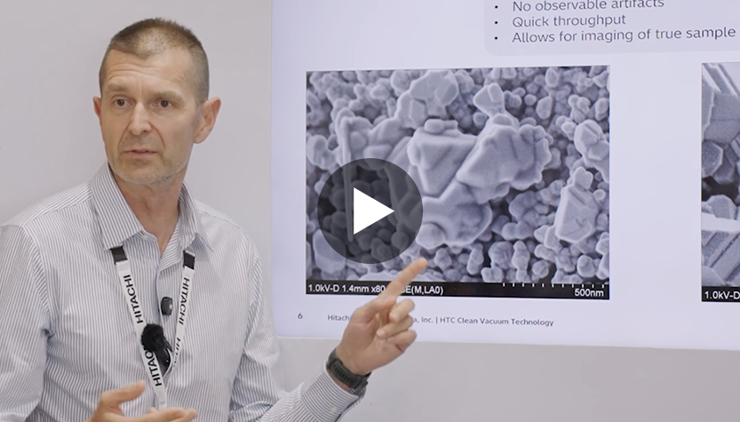
Clean Samples, Better Data: Smart Contamination Control for SEM and TEM
Stas Dogel PhD, NAPG Director at Hitachi High-Tech Canada - Booth 149
Recording
What you will learn
- Versatile sample cleaning
- Removing contamination from vacuum chamber
- In-situ SEM/TEM accessories
Details
Hydrocarbon contamination remains a persistent challenge in electron microscopy, impacting image quality, analytical accuracy, and the reliability of experimental results. Hydrocarbon deposition can degrade imaging resolution, interfere with analytical techniques such as EDS, and influence in situ experiments, potentially leading to erroneous data interpretation. Removing hydrocarbons from sample surfaces without altering their morphology or chemistry is a complex task, while preventing contamination from the microscope vacuum environment presents an additional challenge.
This presentation will explore advanced yet practical solutions for mitigating hydrocarbon contamination in both SEM and TEM applications. Topics will include effective sample cleaning methods, contamination control strategies, and approaches to maintaining clean operating conditions. These techniques can significantly improve imaging performance, analytical reliability, and confidence in experimental outcomes.
In addition, we will showcase a range of SEM and TEM accessories that expand the capabilities of Hitachi electron microscopes. These solutions enhance imaging, analysis, and workflow flexibility, enabling researchers to address a broad spectrum of materials characterization challenges more effectively.
Bio
2000: Metallurgical Engineer Degree
2004: PhD in Chemistry (physical chemistry)
2004-2009: Postdoc (vacuum, physics, surface science)
2009-2011: Staff Scientist in Research Council of Canada
2012-now: Hitachi High-Tech Canada
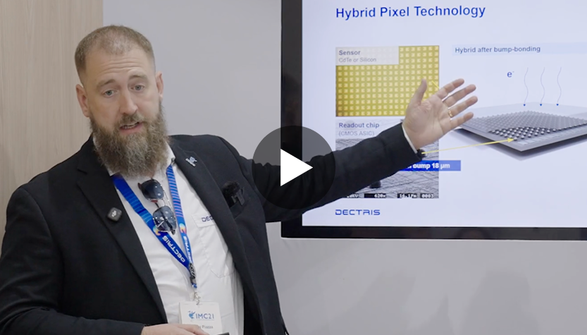
Hybrid-Pixel Detectors for Electron Microscopy
Luca Piazza, Senior Product Manager EM at Dectris - Booth 149
Recording
What you will learn
- What are Hybrid Pixel detectors?
- What are the benefits of this technology?
- Which applications and techniques does it enable.
Details
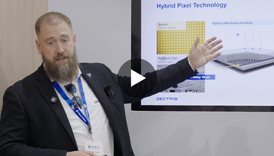
Hybrid-pixel detectors have revolutionized electron microscopy by combining direct detection with noise-free readout and single-electron sensitivity. This technology enables ultrafast 4D STEM at 120,000 frames per second and high-resolution EELS, allowing for the visualization of beam-sensitive materials and complex magnetic domains. By integrating high dynamic range with radiation-hard designs, Hybrid-pixel detectors bridge the gap between traditional imaging and advanced diffraction analysis to empower breakthroughs in materials science and structural biology.
Bio
Originally from Italy, I studied Solid State Physics in Trieste, and I obtained my PhD at EPFL in Switzerland, working with the pioneers in the field of Ultrafast Electron Microscopy. Since 2018 I work in DECTRIS, and I accompanied the company in the journey to develop the first product line of electron detectors to enter the electron microscopy market.
When Electrons Escape: Schottky vs. Cold Field Emission
Dr. Joshua Spille, Applications Specialist OPC at Hitachi High Tech Europe GmbH - Booth 149
More Details Soon
Wednesday 2nd September
SEM Imaging of B-doped Diamond Film by Secondary Electron Energy Filtering
Yoichiro Hashimoto, Senior Engineer at Hitachi High-Tech Corporation- Booth 149
More Details Soon
Visualizing Materials Reactions In-Situ from Ultra-high Vacuum to Near Atmospheric Pressure
Professor Frances M. Ross, (MIT) Massachusetts Institute of Technology
Lunchtime Workshop - Room 20/21
Bio
Frances M. Ross is a faculty member at the Department of Materials Science and Engineering at the Massachusetts Institute of Technology in Cambridge, MA, USA. She received her B.A. in Physics and Ph.D. in Materials Science from Cambridge University, UK, and along the way became an enthusiast of electron microscopy. She extended her interests to include in situ microscopy during her postdoc at A.T.&T. Bell Laboratories, then as a Staff Scientist at the National Center for Electron Microscopy, Lawrence Berkeley National Laboratory, and finally as a Research Staff Member at the IBM T. J. Watson Research Center, before joining MIT. Her research is based around the development of in situ electron microscopy techniques to help understand crystal growth, epitaxy, self-assembly and electrochemical and other liquid phase processes.
Hybrid-Pixel Detectors for Electron Microscopy
Luca Piazza, Senior Product Manager EM at Dectris - Booth 149
Recording
What you will learn
- What are Hybrid Pixel detectors?
- What are the benefits of this technology?
- Which applications and techniques does it enable.
Details
Hybrid-pixel detectors have revolutionized electron microscopy by combining direct detection with noise-free readout and single-electron sensitivity. This technology enables ultrafast 4D STEM at 120,000 frames per second and high-resolution EELS, allowing for the visualization of beam-sensitive materials and complex magnetic domains. By integrating high dynamic range with radiation-hard designs, Hybrid-pixel detectors bridge the gap between traditional imaging and advanced diffraction analysis to empower breakthroughs in materials science and structural biology.
Bio
Originally from Italy, I studied Solid State Physics in Trieste, and I obtained my PhD at EPFL in Switzerland, working with the pioneers in the field of Ultrafast Electron Microscopy. Since 2018 I work in DECTRIS, and I accompanied the company in the journey to develop the first product line of electron detectors to enter the electron microscopy market.
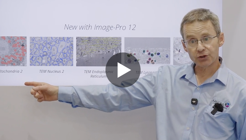
Overcome EM Imaging Challenges with New AI-Powered Enhancement and Segmentation
Andrew Barlow PhD, Product Owner at Media Cybernetics - Booth 149
What you will learn
- Improve EM image quality with AI
- Segment challenging structures faster
- Connect acquisition to automated analysis
Details
Electron microscopy continues to generate larger and more complex datasets, creating new challenges for image quality, segmentation, and efficient analysis. This presentation introduces new capabilities in Image-Pro 12 designed to help researchers move from EM images to reliable quantitative results faster and with greater consistency.
New AI-powered tools address several common barriers in EM workflows. AI Enhance uses deep learning to improve image quality, including compensation for noise associated with short dwell-time acquisition, helping researchers acquire usable images faster while preserving important structural information. AI Hover provides a new interactive approach to segmentation, allowing users to rapidly identify and segment structures of interest with minimal setup. Additional enhancements throughout Image-Pro 12 streamline segmentation, measurement, visualization, and repeatable image analysis workflows.
The presentation will also explore how Image-Pro can extend beyond the desktop through its Python API. In combination with Hitachi’s EM Flow Connector, researchers can integrate Image-Pro image processing and analysis capabilities into automated EM workflows, creating new opportunities to connect image acquisition directly with enhancement, segmentation, measurement, and downstream data processing.
Together, these advances demonstrate how AI and workflow integration can reduce manual effort, improve consistency, and accelerate quantitative analysis of electron microscopy images.
Bio
Andrew Barlow, PhD, is Product Owner at Media Cybernetics, where he helps lead the development of Image-Pro scientific imaging software. With extensive experience in microscopy, image analysis, and quantitative imaging, Andrew works closely with leading research laboratories to understand real-world imaging challenges and translate them into new software capabilities. His work focuses on developing and testing innovative tools that make image analysis more efficient, accurate, and accessible to researchers.
Advanced In-situ Environmental S/TEM for Catalysts and Energy Materials
Hiroaki Matsumoto, Senior Engineer at Hitachi High-Tech Corporation - Booth 149
What you will learn
- Overview of 200kV Cold-FEG Cs-corrected Environmental (S)TEM
- Oxidation and reduction of perovskite electrocatalyst for SOEC
- H2 and CO2 reaction of MoS2 monolayer sheet
Details
In-situ observation of chemical reactions using environmental transmission electron microscopy (TEM) and scanning transmission electron microscopy (STEM) is an effective approach for understanding reaction mechanisms in catalysts and other energy-related materials.
The HF5000 is a 200 kV environmental TEM/STEM equipped with a cold field-emission gun, a probe aberration corrector, and EDS/EELS analytical capabilities, enabling atomic-scale structural and chemical characterization. A differential pumping system allows gas introduction of up to several hundred pascals around the specimen while maintaining imaging performance. In combination with a MEMS-based heating holder capable of rapid heating to 1100 °C, the system enables observation under realistic reaction conditions.
This presentation introduces recent in-situ studies of catalytic materials during oxidation and reduction reactions. The results provide insights into nanoscale structural and chemical changes, reaction mechanisms, and degradation processes, demonstrating the HF5000 as a powerful “lab-in-gap” platform for catalyst and energy-material research.
Bio
Thursday 3rd September
FIB vs BIB: Selecting the Right Approach for the Length Scale
Dr. Justyna Grzonka, Senior Applications Specialist OPC at Hitachi High Tech Europe GmbH - Booth 149
More Details Soon
Strategies for Applying 4D-STEM and Ptychography from 20 to 300 keV
Professor Arthur Blackburn, University of Victoria
Lunchtime Workshop - Room 20/21
What you will learn
- Strategies for acquiring 4D-STEM data for ptychography on Hitachi Electron Microscopes.
- Methods of processing the acquired data to form ptychographic reconstructions.
- About the insights provided from the reconstruction and other 4D-STEM analysis.
Details
Four-Dimensional Scanning Transmission Electron Microscopy (4D-STEM) and electron ptychography are transforming electron microscopy by allowing atomic resolution insights from low energy (≤ 30 keV) scanning electron microscopy (SEM) which rivals or complements the information obtainable from much higher energy aberration corrected instruments. For example, a resolution of at least 0.67 Å has recently been demonstrated using ptychography with a 20 keV electron beam operating in a transmission mode using a SEM with a cold emission gun and immersion lens1. This was realized through combination of adding a diffraction projector lens to our SEM; using an un-coated hybrid direct electron detector2; and incorporating correction of diffraction projector distortions3 within a multi-slice ptychographic reconstruction process. Here I will discuss the strategies we have used to practically collect and process 4D-STEM data for a range of applications and analyses, including ptychography, within our research facility. Applying these techniques to data collected in smaller and lower energy SEM type instruments reduces the need for observations traditionally performed in higher energy instruments and thus widens the access to atomic resolution insights.
1Blackburn, A. M., et al, Nature Communications 16, 8977 (2025); 2Tinti, G., et al., Journal of Synchrotron Radiation 24, 963-974 (2017); 3Fitzpatrick, M. R. C., et al., Ultramicroscopy 283, 114347 (2026).
Bio
Arthur Blackburn holds the Hitachi High-Tech Canada Research Chair in Advanced Electron Microscopy at the University of Victoria, where he directs the Advanced Microscopy Facility and is an Associate Professor in the Department of Physics and Astronomy. Prior to joining the University of Victoria, he was a Senior Research Scientist in the Hitachi Cambridge Laboratory, embedded with the Cavendish Laboratory of the University of Cambridge. He progressed to this role after completing his PhD within the University of Cambridge, Department of Physics.

Overcome EM Imaging Challenges with New AI-Powered Enhancement and Segmentation
Andrew Barlow PhD, Product Owner at Media Cybernetics - Booth 149
What you will learn
- Improve EM image quality with AI
- Segment challenging structures faster
- Connect acquisition to automated analysis
Details
Electron microscopy continues to generate larger and more complex datasets, creating new challenges for image quality, segmentation, and efficient analysis. This presentation introduces new capabilities in Image-Pro 12 designed to help researchers move from EM images to reliable quantitative results faster and with greater consistency.
New AI-powered tools address several common barriers in EM workflows. AI Enhance uses deep learning to improve image quality, including compensation for noise associated with short dwell-time acquisition, helping researchers acquire usable images faster while preserving important structural information. AI Hover provides a new interactive approach to segmentation, allowing users to rapidly identify and segment structures of interest with minimal setup. Additional enhancements throughout Image-Pro 12 streamline segmentation, measurement, visualization, and repeatable image analysis workflows.
The presentation will also explore how Image-Pro can extend beyond the desktop through its Python API. In combination with Hitachi’s EM Flow Connector, researchers can integrate Image-Pro image processing and analysis capabilities into automated EM workflows, creating new opportunities to connect image acquisition directly with enhancement, segmentation, measurement, and downstream data processing.
Together, these advances demonstrate how AI and workflow integration can reduce manual effort, improve consistency, and accelerate quantitative analysis of electron microscopy images.
Bio
Andrew Barlow, PhD, is Product Owner at Media Cybernetics, where he helps lead the development of Image-Pro scientific imaging software. With extensive experience in microscopy, image analysis, and quantitative imaging, Andrew works closely with leading research laboratories to understand real-world imaging challenges and translate them into new software capabilities. His work focuses on developing and testing innovative tools that make image analysis more efficient, accurate, and accessible to researchers.
Automated High-Temperature In-situ TEM Observation Using EM Flow Creator
Toshie Yaguchi, TEM Applications Engineer at Hitachi High-Tech Corporation - Booth 149
What you will learn
- Automated high-temperature in-situ TEM using EM Flow Creator.
- Reproducible acquisition of TEM images and diffraction patterns during heating.
- Thickness-dependent grain-growth behavior in Al and Ni thin films.
Details
High-temperature in-situ transmission electron microscopy (TEM) is a powerful technique for investigating microstructural evolution during thermal processing. However, systematic experiments under multiple temperature conditions often require repetitive and time-consuming manual operations, which can reduce experimental efficiency and reproducibility. In this work, automation of high-temperature in-situ TEM observation was investigated using Hitachi's EM Flow Creator (EMFC) integrated with an HT7800II 120 kV TEM and a MEMS-based heating system. The automated workflow controlled specimen positioning, field alignment, TEM image acquisition, and electron diffraction (ED) pattern collection throughout programmed heating sequences.
The approach was applied to aluminum and nickel thin-film specimens with different initial thicknesses. Temperature-dependent TEM images and ED patterns were automatically acquired during heating up to 400 °C for Al and 700 °C for Ni. The results revealed progressive grain growth with increasing temperature, consistent with enhanced atomic diffusion and grain-boundary migration. Furthermore, specimen thickness significantly affected grain-growth behavior, with thicker specimens exhibiting more pronounced grain coarsening than thinner specimens.
The automated workflow enabled reproducible acquisition of large datasets from identical observation regions while substantially reducing operator intervention. These results demonstrate that EMFC provides an efficient and reliable platform for high-throughput in-situ TEM studies of thermally induced microstructural evolution.
Bio
Toshie Yaguchi is a TEM Applications Engineer at Hitachi High-Tech Corporation, specializing in transmission electron microscopy (TEM), scanning TEM (STEM), and focused ion beam (FIB) technologies. Since joining Hitachi in 1986, she has advanced materials analysis through innovative TEM sample preparation and in-situ observation techniques. She contributed to developing low-damage FIB methods, a semiconductor evaluation system integrating FIB and STEM/SEM, and environmental TEM with enhanced differential pumping. Earning her Ph.D. in 2001, she has led efforts in analytical electron microscopy for beam-sensitive materials. Currently, her primary focus is on advancing in-situ TEM technologies using transmission electron microscopes.