

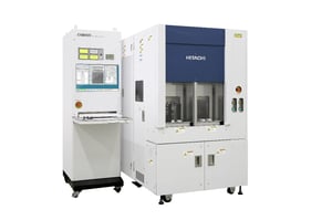
CDSEM CS5000
Hitachi CDSEM CS5000 – advanced Critical Dimension (CD) metrology SEM for reliable, fast, and fully automated measurements on wafers from 75mm to 200mm size.
The Hitachi CS5000 is designed to perform measurements of structures on various substrate materials. Its unique optics modes allow the imaging and measurements even on highly charging wafers. The CS5000 is used in high volume manufacturing sites as well as in research facilities, which require a high degree of flexibility. The small footprint allows installation in facilities with limited clean room space.
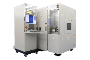
CT1000
Hitachi CT1000 – Advanced 3D SEM for automated, high-resolution Defect Review and Pattern Fidelity Evaluation on wafers from 100mm to 200mm size.
The Hitachi CT1000 is a scanning electron microscope (SEM) that automatically images structures and defects at or near the wafer surface under top-down and tilted view. The integrated energy-dispersive X-ray detector enables the chemical characterisation of defects. The CT1000 is used during the process development phase to facilitate a rapid ramp-up and for defect control to ensure high yield and process quality. Thanks to its small footprint, it can be installed even in facilities with limited cleanroom space.
SU9600 (T)SEM
This new-concept instrument is a modular platform for advanced nanomaterials analysis. Bridging the gap between SEM and TEM, the SU9600 provides unique capabilities by combining SEM & STEM imaging, diffraction, EELS, nano-EDS and 4D-STEM together in one high-stability instrument. Perform routine STEM analysis or complex, multi-modal material investigations quicker than ever before. Explore the exciting low-voltage regime below 30kV, all whilst keeping the flexibility of the world’s highest resolution SEM.
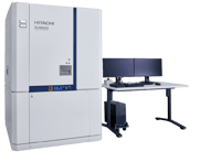
SU8600
A dedicated imaging SEM offering ultra-high resolution thanks to Hitachi’s cold field emission (CFE) technology. Designed to meet the needs of research scientists, lab managers, and industrial users alike, the SU8600 CFE-SEM delivers excellent spatial resolution and automation for modern labs.
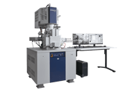
SU8700
An exceptional balance between ultra high-resolution imaging and analytical capabilities, with the ability to handle a wide range of applications. Load samples through a standard six-inch specimen exchange chamber, eventually with an optional inert-gas transfer mechanism and achieve resolution down to 0.6 nm.
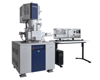
SU3900SE
Featuring a tungsten hairpin filament for reliable, consistent imaging, the Hitachi SU3900 SEM is designed to handle large samples with ease. It accommodates samples up to 5 kg in weight, 300 mm in diameter, and 130 mm in height, while EM-Flow Creator automation ensures smooth, efficient workflows.
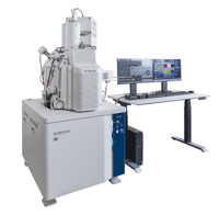
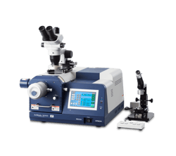
IM5000
High-precision sample preparation for scanning electron microscopy, the IM5000 Broad Ion Beam milling system cuts through hard/soft, mixed, and heat-sensitive materials with near-zero artefacts.
Overcome the speed limitations of your FIB and reveal low damage cross-sections up to 40mm wide, giving you more data for more reliable analysis.

Jürgen Simon
Manager OPC Sales Germany & Italy, Hitachi High-Tech Europe
Jürgen is a physicist specialised in electron microscopy who moved from research at the University of Bonn into microanalysis sales. For the past eight years he has been managing the electron microscope business in Germany and Italy at Hitachi High-Tech Europe.


Stephan Wahl
Expert IPC Sales & Applications Europe, Hitachi High-Tech Europe
Stephan is a physicist with the background of electron microscopy in material science. He joined Hitachi High-Tech Europe 28 years ago as application specialist for semiconductor metrology. During this time he could gain fundamental knowledge about metrology requirements and use his expertise to support customers all over Europe.