Speak to our experts
Explore how the SU3800SE and SU3900SE can help you unlock new levels of precision and efficiency in your scientific research, streamline workflows, level operator capability differences, and reduce workload.
Learn moreHitachi High-Tech Europe
4 min read
Hitachi High-Tech recently launched the SU3800SE and SU3900SE scanning electron microscopes (SEMs). They build upon the field-proven SU3800 and SU3900 instruments, now offering an application-needs optimised instrument in 2 specimen chamber sizes, and a choice between a thermal tungsten or Schottky field emitter.
The new, advanced Field Emission Optics instruments are set to significantly enhance scientific research and industrial applications. With a focus on productivity, the SU3800SE and SU3900SE automate critical optics alignment and repetitive operational tasks, so you can achieve reproducible results in a short time with little manual effort.
As the demand for high-resolution imaging continues to grow across various sectors—including nanotechnology and industrial quality control—these new models will empower researchers and manufacturers to achieve greater insights and improvements in material analysis.
With these advancements, Hitachi High-Tech reaffirms its commitment to supporting groundbreaking discoveries and enhancing product quality across multiple fields.

Scanning electron microscopy has become an indispensable tool in materials research and production control. The technique enables high-resolution surface topography and composition imaging of bulk or particle / filter samples.
But the growing demand for advanced microscopy techniques has created a need for more sophisticated instruments. These instruments must be capable of handling larger and heavier specimens while still maintaining exceptional image quality and ease of use.
Many existing SEMs are limited in their ability to accommodate large, heavy samples. They often need extra specimen preparation such as cutting, which is neither desired nor feasible. Also, the increasing use of SEMs for controlling microstructures to improve material functionality and performance, as well as for analysing foreign matter, faults, and defects to enhance product quality, has highlighted the need for more versatile tools.
Integrating energy dispersive X-ray spectroscopy (EDS) and electron backscatter diffraction (EBSD) help users perform comprehensive material analysis, from elemental composition mapping with EDS to crystallographic orientation studies with EBSD. The growing demand for these capabilities underscores the need for SEMs that can efficiently handle complex, large-scale industrial specimens, like vehicle components, while providing high-resolution imaging and reliable data acquisition.
The SU3800SE and SU3900SE SEMs from Hitachi High-Tech address the above challenges. They come with a number of features and benefits that make your life easier.
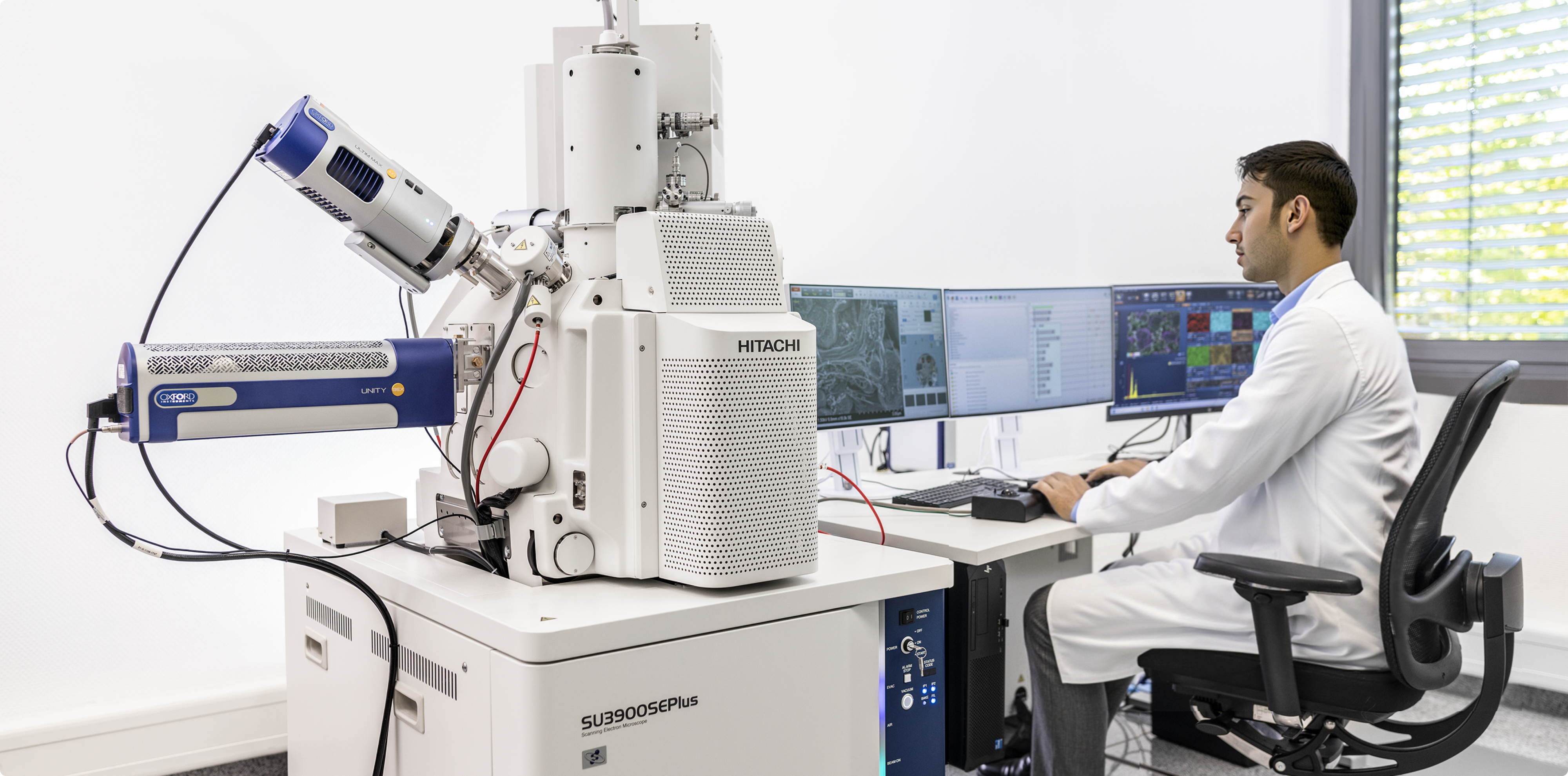
1. Large, heavy, or multi-specimen handling abilityOne of the standout features of the SU3800SE, and especially the SU3900SE, is their ability to handle larger bulk samples on their 5-axes eucentric specimen stages. The SU3900SE can handle specimens up to 300 mm in diameter, 130 mm in height, and 5 kg in weight—with all 5 stage axes being available. This capability reduces or eliminates the need to cut-down larger test items, and it enhances productivity by allowing the loading of multiple specimens for sequential analysis at once.

Samples up to 300mm diameter can be fully inspected (SU3900SE)
2. Effortless and safe sample navigation
These new SEMs also feature an advanced optical camera navigation system that covers the entire range of X,Y stage motion, enabling you to easily locate and access specific specimen positions with a simple mouse-click onto the target position. The optical camera even follows the rotation of the stage, making sample navigation a seamless experience—ideal for users who need to conduct complex and detailed analysis.
Another highlight is the automatically applied sample & stage collision model providing absolute certainty that any available stage motion won’t result in any risk. This allows you to take advantage of the SEM’s full capability e.g. the shortest working distance for highest resolution can be set without any hesitation.
3. Best system performance routinely achievable
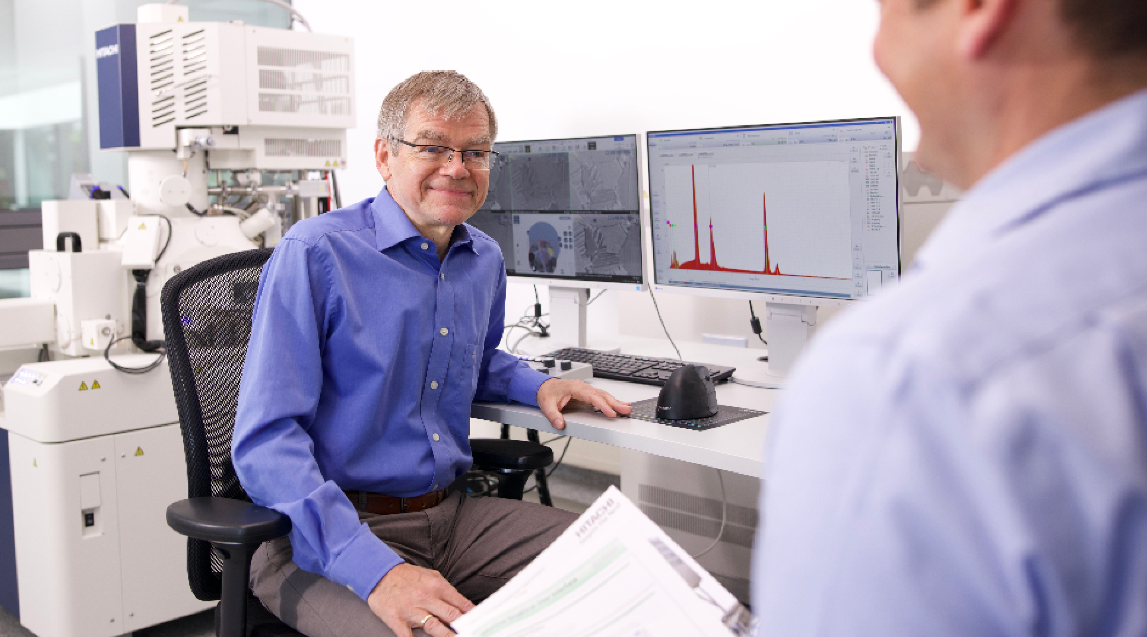
The SU3800SE / SU3900SE come with fast, modular, reliable, and accurate automatic functions for electron optics alignment, focusing, anti-stigmation, and brightness / contrast settings. On top of the user-definable observation condition recipe library, those functions ensure users with different skills consistently output high-quality images, thanks to the high-performance electron optics and detection technology.
4. EM Flow Creator
Repeating routine inspection tasks should not bind an operator to the SEM. The SU3800SE / SU3900SE offer the optional EM Flow Creator function, enabling the setting up of complex workflows without programming or coding skills. EM Flow Creator does this by lining up graphically defined function blocks such as magnification, stage position, image adjustment functions like focus and contrast, and combines them with functions like decision-making events, repeating loops, pattern matching etc. Once set, these recipes can be executed automatically, reducing your workload and ensuring consistent, high-quality results every time.
Bottom line: These benefits mean you’re able to focus on your research, while the microscope takes care of the complex tasks. These SEMs automate processes and ensure accurate, high-quality results with minimal manual intervention on your part.
The introduction of Hitachi's SU3800SE and SU3900SE marks a leap in microscopy technology, with wide-ranging applications across multiple fields.
Nanotechnology
In nanotechnology, where precision at the nanoscale is paramount, these new SEMs help researchers observe and analyse nanostructures with remarkable detail. The high-resolution imaging capabilities allow for the characterisation of nanomaterials, enabling scientists to explore their unique properties and potential applications in electronics, medicine, and materials science.
Industrial quality control
For industrial applications, particularly in quality control, these advanced SEMs allow manufacturers to conduct thorough inspections of materials and components. By identifying defects and analysing microstructures, companies can improve product quality and performance, reducing waste and enhancing efficiency.
The design of the SU3800SE and SU3900SE accommodates larger specimens and offers high-quality imaging of conductive and (through applying the standard-provided variable chamber pressure mode) of non-conductive samples. So you get comprehensive analysis of industrial materials, such as metals, composites, and vehicle parts, without the need for additional processing.
Materials science
In materials science, the new models support critical research in understanding the properties and behaviors of various materials. Their enhanced imaging capabilities enable the examination of surface topography and composition, providing insights that drive innovation in material development. This is particularly important in the development of advanced materials for aerospace, automotive, and electronics industries, where performance and reliability are essential.

LiB cathode material - Distributions of cathode material particles and surrounding binder can be seen
Hitachi's SU3800SE and SU3900SE scanning electron microscopes represent a significant step forward in microscopy.
With their ability to handle larger specimens, advanced automation features, and user-friendly design, these SEMs are set to become essential tools for both industrial and academic users. They improve the efficiency and accuracy of microscopy, and also future-proof labs by providing the flexibility needed to adapt to evolving research and production demands.
If you’re interested in learning more about how these new microscopes can benefit your work, download the brochure or request a demo today. Explore how the SU3800SE and SU3900SE can help you unlock new levels of precision and efficiency in your scientific research.