3 min read
Exploring the benefits of Hitachi’s SU8600 and SU8700 Field Emission SEMs
Mar 15, 2024 12:54:15 PM
In recent decades, the Field Emission SEM (FE-SEM) has emerged as a lynchpin of analytical science, providing professionals in nearly every scientific and engineering field with several benefits over conventional SEMs and allowing them to understand a plethora of complex processes and emerging technologies. Today, we are talking to Roland Schmidt, Senior Applications Specialist, about this innovative technology and Hitachi’s range of FE-SEM microscopes.
What is a Field Emission Scanning Electron Microscope?
The most common types of electron sources for a Scanning Electron Microscope (SEM) are Tungsten or thermionic, Schottky Field Emission and Cold Field Emission (CFE) sources. So, a Field Emission SEM is a SEM equipped with a FE gun. Nowadays, these microscopes provide the best performance in terms of resolution, detection strategy, analytical capabilities and beam stability.
Is Hitachi offering cold-field emission and Schottky field emission scanning microscopes?
That’s right! And to my knowledge, Hitachi is the only company on the market offering SEMs with both Cold Field- and Schottky Emitters.

What benefits can customers expect when using the SU8600 Microscope range?
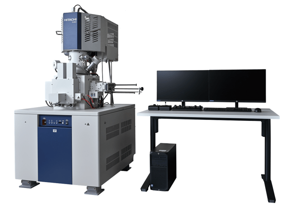
The SU8600 is the latest Cold Field Emission SEM from Hitachi, combining the most advanced imaging modes with three in-lens detectors and EDX detectors which can reach a lateral resolution down to 10nm.
All SU8600 users can take advantage of Hitachi’s profound experience in manufacturing FE-SEMs since the launch of the first CFE-SEM in 1972. In 2012, Hitachi received the renowned IEEE award for continued innovations in this field with over 9000 installed units.
What benefits can academia and industry gain from using the S8600 microscope series?
In industry and academia, maintenance costs and availability of equipment are important concerns. Due to the (theoretical) unlimited lifetime of a cold field emission source, the down time due to tip exchange in an SU8600 is minimal. Indeed, many CFE SEM users have not changed their emitter after more than fifteen years. That really pays off in the long run.
We also see that many customers use the SU8600 as a 30kV Transmission Electron Microscope, combining the advantages of a SEM, especially as a through-the-lens detector, with those of a TEM.
How does the SU8600 series compare to other competitors?
In terms of benefits such as excellent imaging performance, longest tip life, and lowest emission currents starting from 1 µA, there is no competitive model on the market today.
However, many applications may have specific needs. These could include, for example, higher currents, a draw out chamber door, or a Variable Pressure mode to accommodate a wider and potentially unknown sample range. For some applications, a Schottky Emitter may be more convenient.
I am pleased that Hitachi, with the launch of the SU8600 and SU8700, can now offer two FE-SEMs with the same operation, software, and automation features but very different electron optics, with each having its own distinct advantages.
As an Electron Microscopy expert, what is your favourite feature and why?
As mentioned above, our FE-SEMs are as easy to use as Transmission Electron Microscopes. I like that, probably because I started electron microscopy during my PhD on a more sophisticated 300kV TEM. Combining the SEM with the TEM features opens new insights into many nanoscale products such as powders, fibres, carbon nanotubes, and so forth.
Moving onto the SU8700, what benefits can customers expect?
In our FE-SEM product line, the SU8700 and the SU7000 are our all-rounders. They offer the highest flexibility in terms of imaging and vacuum modes, which need chambers with multiple ports for accessories and stable currents up to 200nA.
What sectors and industries can benefit from using the SU8700 Microscope series?
All sectors and industries where the highest flexibility is required to solve the problems of failure analysis and process control in a short time. For example, in the chemical industry, where product cycles are rather short and materials change with higher frequency, and in sectors such as the semiconductor industry.
What is your advice to businesses who do not know which of the two different technologies they should choose?
Get in touch with us to submit a sample. Based on your requirements and needs, we can recommend which of our wide range of microscopes would be the best fit.
Finally, do you have a ‘tip of the month’?
For fixing bulk samples, don’t use double sided carbon tapes for getting high resolution images above 20,000x magnification.
Roland Schmidt
Senior Applications Specialist